What are MEMS?
MEMS/NEMS (Micro-Electro-Mechanical System / Nano–Electro-Mechanical System) are the merger of the integrated circuits (IC), i.e. electronics world, with the mechanical world. Using established IC fabrication processing techniques, along with additional materials from chemical and mechanical processes, it is possible to realize micrometer and nanometer structures for a variety of devices. These devices bridge the gap between the “electrical and mechanical world” and the real, physical world at the micrometer and nanoscale level. This allows the realizations of the micro- and nano-sensors and actuators with their integrated circuitry for a variety of applications at un-precedented levels. Biomedical devices are realized at the micrometer and nanometer scales for applications such as implanted devices in the human body for the continuous monitoring of human health parameters, and for applications such as drug delivery. This allows for the possibility of personalized healthcare.
Importance of MEMS/NEMS
Micro/nanoelectromechanical systems (MEMS/NEMS) technology offers the opportunity to produce mechanical, electromechanical, and electrochemical devices with the same unprecedented levels of miniaturization, and functionality as modern Very Large-Scale Integrated Circuits (VLSI). MEMS/NEMS are a rapidly growing segment of the U.S. semiconductor and nanotechnology industry with a multibillion-dollar market expanding over the next decade. This emerging technology utilizes mechanical structures fabricated using the microfabrication techniques, perfected by the semiconductor industry, to perform sensing and actuation functions and realize a variety of devices at the microscale and at the nanoscale. Commercial applications for this technology include pressure sensors, fluid regulation and control, optical switching, mass data storage, chemical and biological sensing and control, and medical devices implanted in the human body. The number of MEMS/NEMS based applications is increasing at a rapid pace, particularly in the field of micro/nano sensors that integrate the MEMS/NEMS structures with signal processing circuits on the same chip to produce smart sensors. The wide spectrum of research topics in this area includes the development of new materials and the use of nanotechnology techniques to push sensors beyond current limitations, such as high temperature devices, submicron medical devices, and new human implanted sensors devices.
Technical Interdisciplinary of the MEMS Research
Manufacturers and users of MEMS/NEMS technology must be able to understand the behavior of those structures and accurately model their behaviors. The design and characterization of MEMS/NEMS devices requires a knowledge of the material properties involved, an awareness of semiconductors circuit design methodology, the mechanical properties of the devices, and the ability to model the devices accurately. MEMS/NEMS device research involves the characterization of MEMS/NEMS material properties which include material residual stresses, thermal expansion, conductivity, mechanical strength, fatigue and fracture resistance, and others. The research in this area spans a wide range of disciplines in electrical engineering, mechanical engineering, material sciences, and applications of MEMS devices in several disciplines. Among these disciplines, the key factor for the rapid progress of microsensors and MEMS has been silicon microfabrication technology and silicon micromachining. This refers to fashioning microscopic mechanical parts out of a silicon substrate or on a silicon substrate. MEMS/NEMS technology requires the knowledge of chemists, physicists, electrical engineers, mechanical engineers, optoelectronics engineers, material scientists, and biomedical engineers. This wide range of interdisciplinary skills is well represented in The George Washington University’s schools, faculty, and institutes.
GWU MEMS/NEMS Mission
The MEMS/NEMS research at GWU is focused on using different technologies combined with pre- and/or post-clean room processing steps. Several devices are realized using semiconductor technology and the clean room facility at The George Washington University. The devices include sensors and smart sensors with integrated electronics, RF MEMS devices, power sensors, surface acoustic wave (SAW) devices for communications and sensor applications, biosensors for medical applications, environmental sensors such as gas sensors, and implanted biomedical devices to monitor human health parameters. The research group uses CMOS to add active circuitry to the sensor, hence creating complete smart systems. The institute enhances research in the areas of MEMS, NEMS, and Integrated Circuits by introducing courses in these areas with recent state of the art topics.
Examples of MEMS/NEMS Devices Developed at GWU
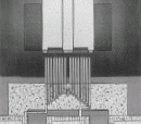
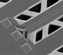
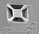
Devices developed over the years by the institute.



- Ritu Bajpai, graduated 2014, currently employed with Apple company at Silicon Valley
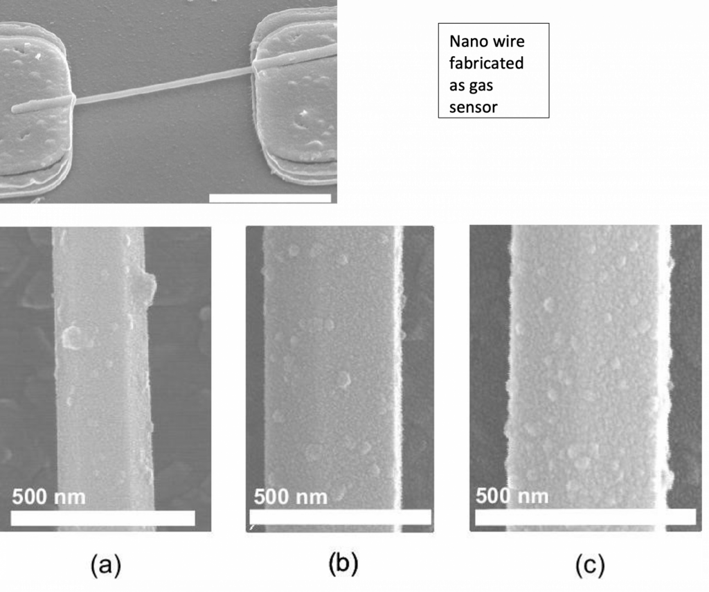
Dr. Bajpai worked with zinc oxide nano particles sputtered on nanowire using a sputtering technique to enhance gas sensing. Dr. Bajpai contributed to 3 U.S. patents and a company was established using these novel techniques.
- Dr. Shiqi Guo, graduated 2019. Dr. Guo is currently working as a post doctorate at Harvard University. While working in the institute, she worked on sensors on human skin, integrating gas sensors onto the skin.
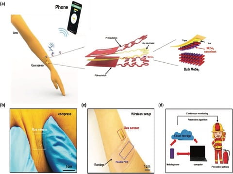
Human skin electronics for the measurement of environmentally toxic gases
- Dr. Yangyang Zhao, graduated 2019. Dr. Zhao is currently starting small business. While working in the institute, he worked with on a nanohole chemical gas sensor, developing a nano-Device for detecting small nanoscale molecules.
Recently GWU received a contract from Hoth Therapeutics in NYC to use the device for detecting Covid-19 virus in human saliva. Professor Zaghloul is the PI for the project to develop a device for detecting the Covid -19 virus for fast point-of-care detection at home.

